
Mutilayer PCB Selective Hard Gold Plating Sideplating Castellated Holes| YSPCB


What is Multilayer PCBs
Multilayer PCBs are built by joining all the number of layers and materials at high temperature and pressure so as to remove any trapped air between the layers. Resin and adhesive material is used to stick the components and different layers together. You can choose from a number of materials such as exotic ceramic, epoxy glass, or Teflon etc. to build your PCB. The different prepreg and core layers are combined and go through the lamination process taking place at high temperature and pressure that helps to melt the layers together. After that the PCB is cooled down to form a hard and solid board.
PCB Sideplating
Sideplating is the metalization of the board edge in the PCB filed. Edge plating, Border plated, plated contour, side metal, these words can also be used to describe the same function.
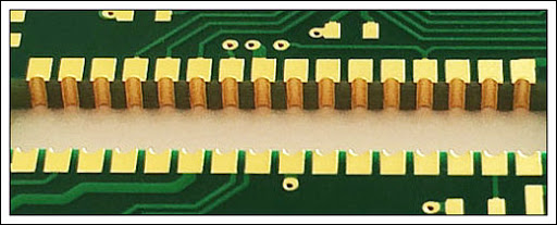
Half-cut Castellated Holes
Castellations are plated through holes or vias located in the edges of a printed circuit board. are indentations created in the form of semi-plated holes on the edges of the PCB boards.These half holes serve as pads intended to create a link between the module board and the board that it will be soldered onto.
YS Multilayer PCB manufacturing capabilities:
| YS Multilayer PCB manufacturing capabilities overview | ||
| Feature | capabilities | |
| Layer Count | 3-60L | |
| Available Multilayer PCB Technology | Through hole with Aspect Ratio 16:1 | |
| buried and blind via | ||
| Hybrid | High Frequency Material such as RO4350B and FR4 Mix etc. | |
| High Speed Material such as M7NE and FR4 Mix etc. | ||
| Thickness | 0.3mm-8mm | |
| Minimum line Width and Space | 0.05mm/0.05mm(2mil/2mil) | |
| BGA PITCH | 0.35mm | |
| Min mechanical Drilled Size | 0.15mm(6mil) | |
| Aspect Ratio for through hole | 16:1 | |
| Surface Finish | HASL, Lead free HASL,ENIG,Immersion Tin, OSP, Immersion Silver, Gold Finger, Electroplating Hard Gold, Selective OSP,ENEPIG.etc. | |
| Via Fill Option | The via is plated and filled with either conductive or non-conductive epoxy then capped and plated over(VIPPO) | |
| Copper filled, silver filled | ||
| Registration | ±4mil | |
| Solder Mask | Green, Red, Yellow, Blue, White, Black, Purple, Matte Black, Matte green.etc. | |
Learn more about YS products

Flex Circuit Board

Rigid flex pcb multilayer FPC

HDI pcb


