
Thick Copper PCB 10 Layer (4OZ) High Tg Full Body Hard Gold (BGA) Board| YS PCB


What is Heavy copper PCB?
Heavy copper PCB products are widely used in power electronic equipment and power supply system.The additional copper PCB thickness enables the board to conduct a higher current, achieve good thermal distribution and implement complex switches in a limited space.
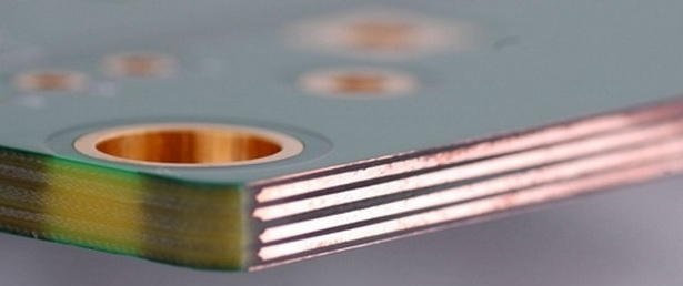
This unique type of thick copper PCB has a finished copper weight of more than 4 ounces (140 microns), compared to the standard PCB copper thickness of 1ozor 2oz.
Usually, the copper thickness of a standard PCB is 1oz to 3oz. Thick-copper PCBs or heavy-copper PCBs are the types of PCBs that the finished copper weight is more than 4oz (140μm). The thick-copper PCB belongs to a special type of PCB. its conductive materials, substrate materials, production process, application fields are different from the conventional PCBs. The plating of thick copper circuits allows PCB manufacturers to increase the copper weight in via sidewalls and plated holes, which can reduce the layer numbers and footprints. Thick-copper plating integrates high-current and control circuits, making high-density with simple board structures can be achieved.Thick copper PCB is widely used in various household appliances, high-tech products, military, medical and other electronic equipment. The application of thick copper PCB makes the core component of electronic equipment products-circuit boards have a longer service life, and at the same time it is very helpful to the size reduction of electronic equipment
In PCB prototype, thick copper PCB belongs to a special technology, has certain technical thresholds and operating difficulties, and is relatively expensive. At present, in the process of PCB prototype, YMS can achieve 1-30 layers, the maximum copper thickness is 13oz, the minimum hole size is 0.15 ~ 0.3mm.The applications of thick-copper PCBs
Along with the increasing of high-power products, the demand for thick-copper PCBs is greatly increased. Today’s PCB manufacturers pay more attention to using a thick copper board to solve the thermal efficiency of high-power electronics.
The thick-copper PCBs are mostly large current substrate, and large current PCBs are mainly used in power module and automotive electronic parts. Traditional automotive, power supply, and power electronics applications use the original forms of transmission like cable distribution and metal sheet. Now the thick-copper boards replace the transmission form, which not only can improve productivity and reduce the time cost of wiring, but also increase the reliability of final products. At the same time, the massive current boards can improve the design freedom of wiring, thus realizing the miniaturization of the whole product.In short, thick-copper circuit PCB play an irreplaceable role in the applications with high-power, high current, and high cooling demand. The manufacturing process and materials of heavy-copper PCBS have much higher requirements than standard PCBs. With advanced equipment and professional engineers, China YMS PCB is a professional manufacturer which can provides thick-copper PCBs with high-quality for customers from home and abroad.
YS Heavy copper PCB manufacturing capabilities:
| YS Heavy copper PCB manufacturing capabilities overview | ||
| Feature | capabilities | |
| Layer Count | 1-30L | |
| Base Material | FR-4 Standard Tg, FR4-mid Tg,FR4-High Tg | |
| Thickness | 0.6 mm - 8.0mm | |
| Maximum Outer Layer Copper Weight (Finished) | 15OZ | |
| Maximum Inner Layer Copper Weight (Finished) | 30OZ | |
| Minimum line Width and Space | 4oz Cu 8mil/8mil; 5oz Cu 10mil/10mil; 6oz Cu 12mil/12mil; 12oz Cu 18mil/28mil; 15oz Cu 30mil/38mil .etc. | |
| BGA PITCH | 0.8mm(32mil) | |
| Min mechanical Drilled Size | 0.25mm(10mil) | |
| Aspect Ratio for through hole | 16:1 | |
| Surface Finish | HASL, Lead free HASL,ENIG,Immersion Tin, OSP, Immersion Silver, Gold Finger, Electroplating Hard Gold, Selective OSP,ENEPIG.etc. | |
| Via Fill Option | The via is plated and filled with either conductive or non-conductive epoxy then capped and plated over(VIPPO) | |
| Copper filled, silver filled | ||
| Registration | ±4mil | |
| Solder Mask | Green, Red, Yellow, Blue, White, Black, Purple, Matte Black, Matte green.etc. | |
Learn more about YS products

Flex PCB 1Layer White

SMD LED display screen pcb

hdi pcb high speed

PCB manufacturing high frequency
Video


