
high-density multilayer pcbs 8L Printed Circuit Board Halogen Free Material| YS


What is Multilayer PCBs
Multilayer Printed Circuit Board, It is a type of PCB which comes with a combination of single sided PCB and double sided PCB. It features layers more than double sided PCB.
Benefits of Multilayer PCBs (compared to single or double-sided PCBs)
Higher assembly density
Smaller size (considerable savings on space)
Increased flexibility
Easier incorporation controlled impedance features.
EMI shielding through careful placement of power and ground layers.
Reduces the need for interconnection wiring harnesses (reduces overall weight)
Building a Multilayer PCB
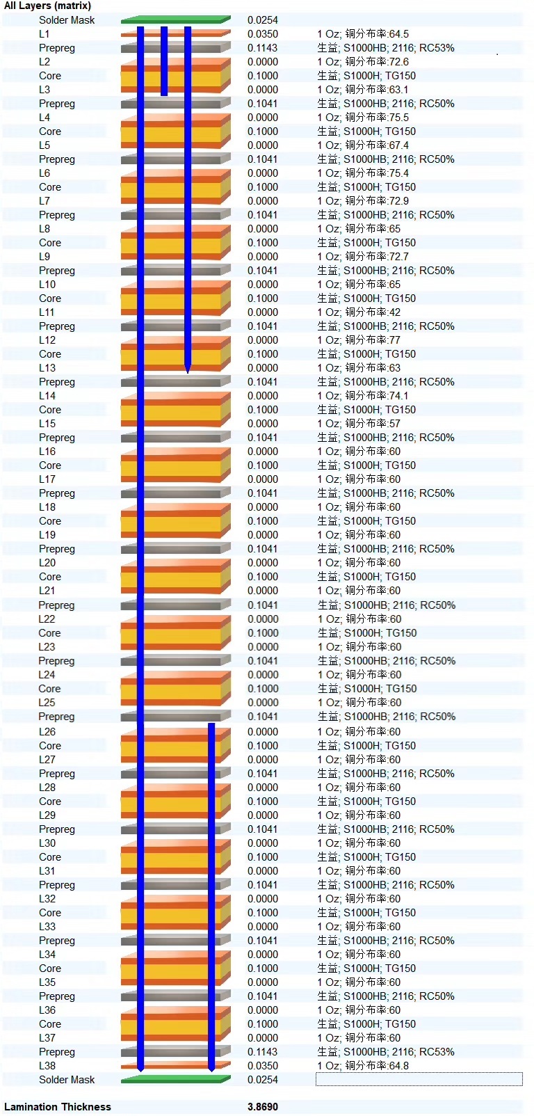
Multilayer PCBs are built by joining all the number of layers and materials at high temperature and pressure so as to remove any trapped air between the layers. Resin and adhesive material is used to stick the components and different layers together. You can choose from a number of materials such as exotic ceramic, epoxy glass, or Teflon etc. to build your PCB. The different prepreg and core layers are combined and go through the lamination process taking place at high temperature and pressure that helps to melt the layers together. After that the PCB is cooled down to form a hard and solid board.
High-density interconnect, or HDI, circuit boards are printed circuit boards with a higher wiring density per unit area than traditional printed circuit boards. In general, HDI PCBs are defined as PCBs with one or all of the following: microvias; blind and buried vias; built-up laminations and high signal performance considerations. Printed circuit board technology has been evolving with changing technology that calls for smaller and faster products. HDI boards are more compact and have smaller vias, pads, copper traces and spaces. As a result, HDIs have denser wiring resulting in lighter weight, more compact, lower layer count PCBs. Rather than using a few PCBs in a device, one HDI board can house the functionality of the previous boards used.
The characteristics of HDI PCBs in designing and manufacturing
HDI PCBs have finer lines, minor holes, and higher density than conventional PCBs, providing necessary touting solutions for the chips with many pins in mobile devices and other high-tech products.
HDI design combines dense component placement and finer circuits, using less board without compromise functions. Compared to ordinary PCBs, the main difference is that HDI PCBs realize the interconnect through blind vias and buried vias instead of through holes. And HDI PCBs use laser drilling while traditional PCBs usually use mechanical drilling. Laser drilling allows smaller apertures whose sizes are in the range of 3.0-6.0mil, which will save much space of the pad, and more layout can be achieved in the unit area.
The advantages and applications of HDI PCBs
· Compact design
The combination of micro vias, blind vias, and buried vias reduces the board space greatly. With the support of HDI technologies, a standard 8-layers through-hole PCB can be simplified to a 4-layer HDI PCB with the same functions.
· Excellent signal integrity
With small vias, all stray capacitance and inductance will get reduced. And the technology of incorporating bind vias and via-in-pad helps to shorten the length of the signal path. These will lead to faster signal transmission and better signal quality.
· High reliability
HDI technology makes route and connect easier, and offers PCBs better durability and reliability in hazardous conditions and extreme environment.
· Cost-effective
There needs much more manufacturing cost when the boards are beyond 8-layer if using traditional pressing processes. But HDI technology can reduce the cost and keep the function purpose.
HDI PCBs have been used widely to reduce the entire size and weight of final products while enhancing the electrical performance. For these medical devices like pacemakers, miniaturized cameras, and implants, only HDI techniques are capable of supplying small packages with fast transmission rates. HDI PCBs are responsible for smaller portable products, such as smartphones, tablets, and wearable electronics. Automotive devices, military, and aerospace equipment also need the support of HDI technologies.
YS Multilayer PCB manufacturing capabilities:
| YS Multilayer PCB manufacturing capabilities overview | ||
| Feature | capabilities | |
| Layer Count | 3-60L | |
| Available Multilayer PCB Technology | Through hole with Aspect Ratio 16:1 | |
| buried and blind via | ||
| Hybrid | High Frequency Material such as RO4350B and FR4 Mix etc. | |
| High Speed Material such as M7NE and FR4 Mix etc. | ||
| Thickness | 0.3mm-8mm | |
| Minimum line Width and Space | 0.05mm/0.05mm(2mil/2mil) | |
| BGA PITCH | 0.35mm | |
| Min mechanical Drilled Size | 0.15mm(6mil) | |
| Aspect Ratio for through hole | 16:1 | |
| Surface Finish | HASL, Lead free HASL,ENIG,Immersion Tin, OSP, Immersion Silver, Gold Finger, Electroplating Hard Gold, Selective OSP,ENEPIG.etc. | |
| Via Fill Option | The via is plated and filled with either conductive or non-conductive epoxy then capped and plated over(VIPPO) | |
| Copper filled, silver filled | ||
| Registration | ±4mil | |
| Solder Mask | Green, Red, Yellow, Blue, White, Black, Purple, Matte Black, Matte green.etc. | |
Video
Learn more about YS products

Flexible PCB Board

Rigid flex pcb design HDI

Multilayer PCBs

Metal clad pcb
Read more news
3. What are flexible circuit boards made of


