
Selective Hard Gold PCB High TG FR4 Material main board| YS PCB


The difference between hard gold and soft gold
Goldplating can be divided into hard gold and soft gold. Because electroplated hard gold is alloy, its hardness is relatively hard, and it is suitable for use in places requiring force and friction. It is generally used as PCB side contact point (commonly known as gold finger). While soft gold is generally used for COB (Chip On Board) On the aluminum wire, or the contact surface of mobile phone keys, has recently been widely used in the BGA Board On both sides.
Glass Transition Temperature (Tg)—This is an important parameter for the base material, as it determines the temperature at which the resin matrix changes over from a firm, non-elastic condition to a soft, elastic one.
The difference between hard gold and soft gold is the composition of the layer of gold that is finally plated. When plating gold, you can choose to electroplate pure gold or alloy, because the hardness of pure gold is soft, so it is also called "soft gold".
Full Body Hard Gold is generally a rarely-chosen surface finish, where the full body of the PCB board is plated with hard gold. In order to apply a Full Body Hard Gold surface finish, an electrolytic process using an electric current or an immersion process is needed, depending on the PCB design.
For Complete PCB Assembly projects, where we fabricate and assemble the boards, we will also need to consider the poor solderability of this finish; a very active flux will be required to solder effectively to the hard-gold-plated pad.
If you have any further questions about our PCB Surface Finish capabilities, or to get started on your project with YMS today, you can Contact Us over email at kell@ymspcb.com.
Parameters
Layers: 8L High Tg FR4 Material
Base Material:IT180A High tg 170°
Thickness:3.2mm
Min Holes:0.25mm
Minimum Line Width/Clearance:0.10mm/0.10mm
Minimum Clearance between Inner Layer PTH to Line: 0.2mm
Size:192mm×135mm
Aspect Ratio:12.8 : 1
Surface treatment:ENIG+Selective Hard Gold Plating
Process characteristics: High tg, Selective hard gold
Applications:Communication
What is high Tg PCB (printed circuit board)
Normally high Tg refers to high heat resistance in PCB raw material, the standard Tg for copper clad laminate is between 130 – 140℃, High Tg is generally greater than 170℃, and middle Tg is generally greater than 150℃. Basically the printed circuit board with Tg≥170℃, we call high Tg PCB.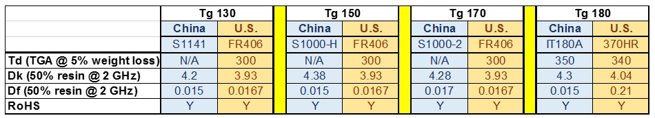
Hard Gold
▪ Usual thickness: 0.7 µm (0.00003”) to 1.3 µm (0.00005”) gold (99.7%) over 5.0
▪ µm (0.0002”) nickel or 0.2 µm (0.000008”) to 0.3 µm (0.00001”) gold (99.7%) over
▪ 5.0 µm (0.0002”) nickel for a solderable surface
▪ Very good for corrosion resistance
▪ Rated at 130-220 Knoop hardness
▪ Very good wear resistance
▪ Excellent for surface rotary switches, on-off contacts, and edge connectors
▪ Very good shelf life
YS High Tg PCB manufacturing capabilities:
YS High Tg PCB manufacturing capabilities overview | ||
| Feature | capabilities | |
| Layer Count | 3-60L | |
| Available Multilayer PCB Technology | Through hole with Aspect Ratio 16:1 | |
| buried and blind via | ||
| Hybrid | High Frequency Material such as RO4350B and FR4 TG 180°Mix etc. | |
| High Speed Material such as M7NE and FR4 TG 180°Mix etc. | ||
| Thickness | 0.3mm-8mm | |
| Minimum line Width and Space | 0.05mm/0.05mm(2mil/2mil) | |
| BGA PITCH | 0.35mm | |
| Min mechanical Drilled Size | 0.15mm(6mil) | |
| Aspect Ratio for through hole | 16:1 | |
| Surface Finish | HASL, Lead free HASL,ENIG,Immersion Tin, OSP, Immersion Silver, Gold Finger, Electroplating Hard Gold, Selective OSP,ENEPIG.etc. | |
| Via Fill Option | The via is plated and filled with either conductive or non-conductive epoxy then capped and plated over(VIPPO) | |
| Copper filled, silver filled | ||
| Registration | ±4mil | |
| Solder Mask | Green, Red, Yellow, Blue, White, Black, Purple, Matte Black, Matte green.etc. | |
Learn more about YS products

Flexible PCB

multilayer flexible pcb

High TG FR4 Material PCB

HDI printed circuit boards
Read more news
1. What to do with gold finger pcb
2. Which kind of PCB board needs gold and goldfinger
4. How to do edge plating on PCB board
5. What is copper plating in PCB


